Hotline:15086707142
 3 / 3
3 / 3
图片三 |
inline-Apcrs |
| Publisher:Shanghai Jinghong Kepu Optoelectronics Technology Co., Ltd. Release time:2025-06-24 10:36:11 Click count:42 Close |
 |
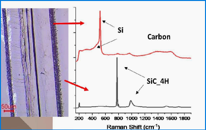
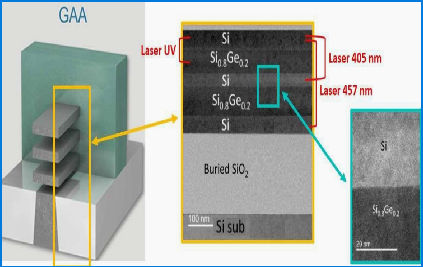
Changes in material structure Specific layer concentration of wafer Wafer cutting process (peak position distribution) Transistor structure process, (chemical bond breaking and decomposition into Si and C) multi-layer silicon germanium alloy concentration, (excessive precipitation of Si and C at high temperature) (peak intensity distribution) (peak shift distribution) |

Shanghai Jinghongkepu Optoelectronics Technology Co., Ltd TEL:15086707142 E-MALI:SHJH@cl-spectrum.com WEB: www.cl-spectrum.com ADD:Building 9, No. 199 Changjian Road, Baoshan District, Shanghai ICP Registration No. 2025109007-1
 Scan the mobile website
 Cell phone station