Hotline:15086707142
 3 / 3
3 / 3
图片三 |
UniDron EFEM-Semi |
| Publisher:Shanghai Jinghong Kepu Optoelectronics Technology Co., Ltd. Release time:2025-06-24 13:26:12 Click count:33 Close |
 |
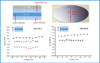 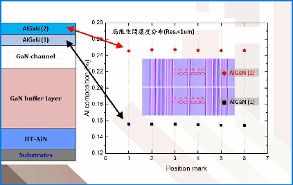
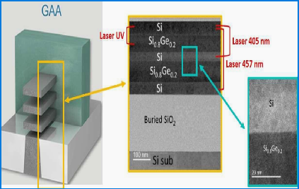
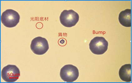
Circular depth multi-layer stress Wafer doping concentration
Thin film deposition process, (positive compressive stress), Double layer aluminum ion implantation process (aluminum doping value)
(negative tensile stress), (spectral peak displacement distribution) (negative tensile stress), (spectral peak displacement distribution)
crystalline imperfection Qualitative analysis of material composition
Substrate stacking faults (FWHM distribution of spectral peaks) Etching process foreign matter
(Residual SiO2 on chip) (Distribution of spectral peak positions)
|

Shanghai Jinghongkepu Optoelectronics Technology Co., Ltd TEL:15086707142 E-MALI:SHJH@cl-spectrum.com WEB: www.cl-spectrum.com ADD:Building 9, No. 199 Changjian Road, Baoshan District, Shanghai ICP Registration No. 2025109007-1
 Scan the mobile website
 Cell phone station
